I have a growing collection of mostly cheap buck/boost converters and am kinda curious about their efficiency and output voltage stability.
Measuring that typically entails varying input voltage and output current while logging input voltage (V_i), input current (I_i), output voltage (V_o), and output current (I_o).
For each reading, efficiency is then defined as (V_o · I_o) / (V_i · I_i) · 100%.
+-------------+
|             |
|    Input    |
|             |
+---+-----+---+
    |     |
    |     +-+
    |      I_i
    |     +-+
    +-V_i-+
    |     |
+---+-----+---+
|             |
|  Converter  |
|    under    |
|    Test     |
|             |
+---+-----+---+
    |     |
    +-V_o-+
    |     +-+
    |      I_o
    |     +-+
    |     |
+---+-----+---+
|             |
|    Output   |
|             |
+-------------+
The professional method of obtaining these values would probably involve a Source/Measure Unit (SMU) with 4-wire sensing and remote control to automatically vary input voltage / output current while logging voltage and current readings to a database. I do not have such a device here -- first, they tend to cost €€€€ or even €€€€€, and second, many of those are more at home in the single-digit Watt range. I do, however, have a lab PSU with remote control and access to output voltage and current readings, a cheap electronic load (without remote control), an ADS1115 16-Bit ADC for voltage measurements, and an ATMega328 for data logging. This allows me to manually set a constant output current I_o and then automatically vary the input voltage while logging V_i, I_i, and V_o.
There is just one catch: The ADS1115 cannot measure voltages that exceed its input voltage (VCC, in this case 5V provided via USB). A voltage divider solves this, at the cost of causing a small current to flow through the divider rather than the buck/boost converter under test. In my case, I only had 10kΩ 1% resistors at hand, and used them to build an 8:1 divider for both differential ADS1115 input channels. This way, I can measure up to 40V, with up to 500µA flowing through the voltage divider. Compared to the 100 mA to several Amperes I intend to use this setup with, that is negligible.
V_i + ----+                  VCC  GND           VCC  GND
         70k                   |  |               |  |
          +--+ +------------+  |  | +-----------+ |  |
         10k +-+A0          +--+  | |           +-+  |
V_i - ----+-+  |            |     | |           |    |
            +--+A1          +-----+ |           +----+
V_o + ----+    |  ADS1115   |       | ATMega328 |
         70k+--+A2       SCL+-------+SCL      TX+--------to USB-Serial converter
          +-+  |            |       |           |
         10k +-+A3       SDA+-------+SDA        |
V_o - ----+--+ +------------+       +-----------+
Of course, this whole contraption is far from certifiably accurate or ppm-safe, and even less so when looking at the real-world setup on my desk.
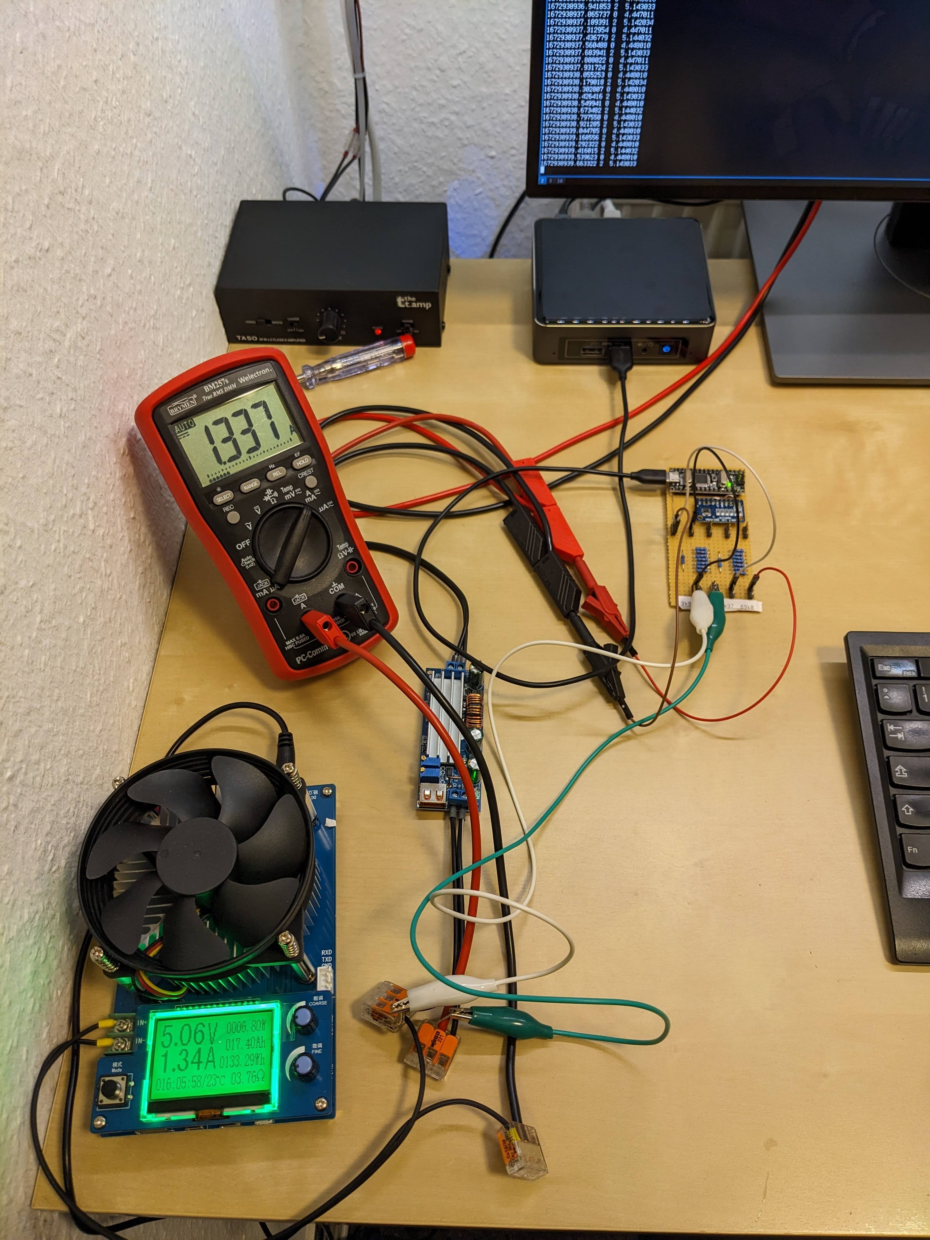
I did however find it to be accurate within ±10mV after some calibration, so it is sufficient to determine whether a converter is in the 80% or 90% efficiency neighbourhood and whether it actually outputs the configured 5.2V or decides to go up to 5.5V under certain load conditions. Luckily, that is all I need.
The bottom line here is: If you have sufficiently simple / low-accuracy requirements, cheap components that may already be lying around in some forgotten project drawer can be quite useful. Also, I really like how easy working with the ADS1115 chip is :)